Graphics Processing Units (GPU) Subsystem Design for SoC Integration
SoC Architecture · RTL & Verification · EDA Methodology
The exponential growth of Artificial Intelligence (AI), Machine Learning (ML), autonomous driving, gaming, high-performance computing, and edge intelligence has significantly transformed the role of Graphics Processing Units (GPUs). Once designed primarily for graphics rendering, GPUs have evolved into highly parallel computing engines capable of accelerating complex mathematical computations across a wide range of applications. As these applications continue to demand higher computational throughput while maintaining stringent power and thermal constraints, GPU subsystem design has become one of the most sophisticated engineering challenges in modern System-on-Chip (SoC) development.
Developing a high-performance GPU subsystem requires much more than implementing RTL for individual functional blocks. It demands architectural planning, performance exploration, virtual prototyping, comprehensive verification, and seamless integration with the complete SoC. This blog discusses a practical approach to GPU subsystem development, the key performance considerations, the growing importance of virtual modeling, commonly used EDA tools, and the complete design methodology leading to successful SoC integration.
GPU Subsystem Architecture
A GPU subsystem is a highly parallel processing engine designed to execute thousands of concurrent threads efficiently. Unlike RISC CPUs, GPUs maximize computational throughput by executing numerous lightweight operations simultaneously. This makes them indispensable in high-performance applications such as graphics rendering, AI inference, computer vision, scientific simulations, digital signal processing, and autonomous systems.
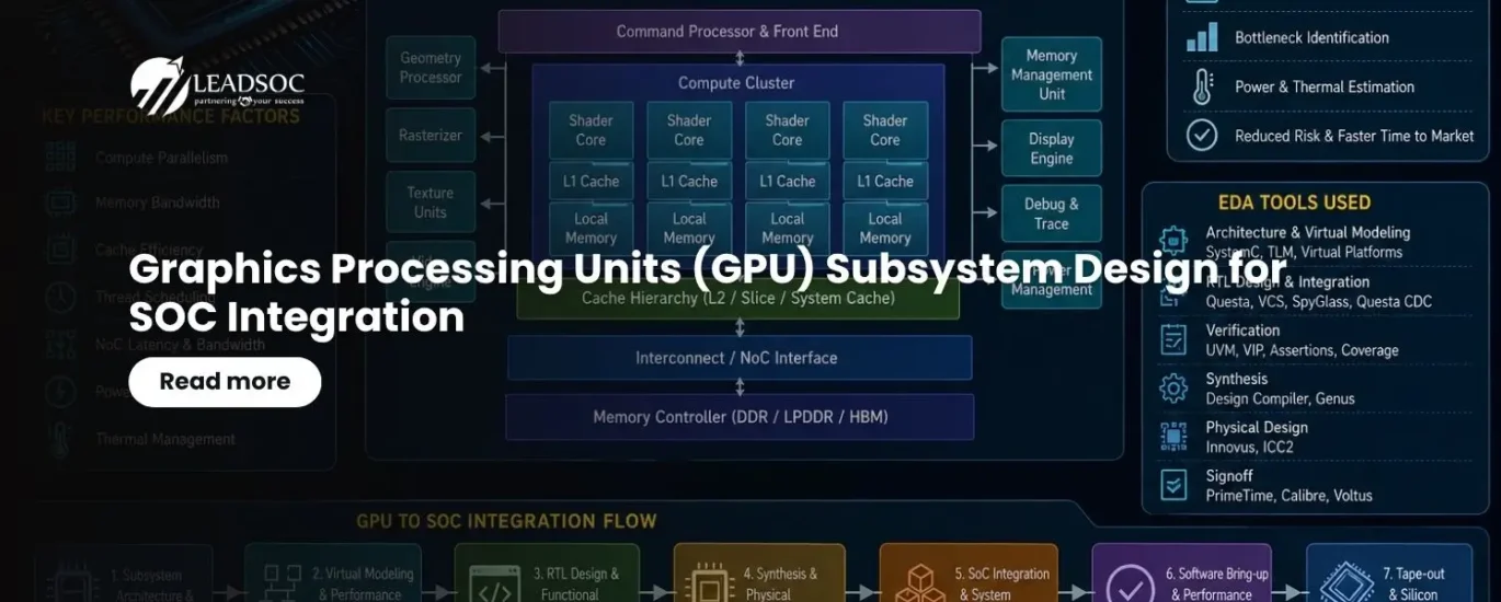
A typical GPU subsystem consists of command processors, shader or compute clusters, instruction schedulers, texture processing units, rasterization engines, cache hierarchy, memory management units, network-on-chip interfaces, performance monitoring blocks, debug infrastructure, and power management logic. These functional blocks operate together to deliver high computational efficiency while sharing system memory and communication resources with processors, AI accelerators, image signal processors, and other SoC components. Designing these subsystems requires balancing computational capability with memory bandwidth, latency, and power consumption to achieve the desired application performance.
A Design Approach to GPU Subsystem
GPU subsystem design begins with understanding the computational requirements of the target application. Whether the target is automotive visualization, industrial AI, cloud computing, consumer graphics, or embedded edge intelligence, the workload characteristics determine the architecture of the subsystem. Designers estimate the required compute throughput, memory bandwidth, cache organization, scheduling mechanisms, and interconnect performance before any RTL modeling.
Once the architectural requirements are finalized, the subsystem is partitioned into multiple functional blocks with clearly defined interfaces. High-level architectural simulations are performed to evaluate different configurations and identify potential bottlenecks. Only after validating the architectural decisions does the development proceed toward RTL implementation, functional verification, synthesis, physical implementation, and complete SoC integration. This structured methodology significantly reduces redesign effort during later stages of development and improves first-silicon success.
GPU Design Performance Factors
The performance of a GPU subsystem depends on the optimization of several interacting architectural parameters. Increasing the number of compute units alone rarely guarantees higher application performance if the memory subsystem cannot deliver sufficient data. Similarly, a high-bandwidth memory interface may remain underutilized if cache efficiency is poor or if interconnect congestion limits data movement.
Designers therefore evaluate computational parallelism, thread scheduling efficiency, cache hierarchy, memory bandwidth utilization, instruction throughput, network-on-chip latency, command processing overhead, and synchronization mechanisms simultaneously. In addition to computational performance, power consumption and thermal behavior play equally important roles, particularly in battery-powered embedded systems and automotive platforms where energy efficiency directly impacts product reliability and operating lifetime.
Modern GPU architecture development is therefore an iterative optimization process in which architectural trade-offs are continuously evaluated until the desired balance between performance, power, area, and cost is achieved.
Importance of Virtual Modeling in GPU Design
One of the greatest challenges in GPU development is discovering architectural bottlenecks after RTL implementation has already started. Correcting such issues at the RTL stage often requires significant redesign effort and delays the overall project schedule. Virtual modeling addresses this problem by enabling architects to evaluate the complete subsystem long before detailed hardware implementation.
Virtual platforms model processors, GPU components, memory systems, caches, interconnects, and software interactions at higher levels of abstraction using transaction-level modeling techniques. These models execute significantly faster than RTL simulations while maintaining sufficient accuracy for architectural evaluation.
Virtual prototypes allow software teams to begin operating systems, driver, middleware, and application development months before silicon is available. At the same time, hardware architects can study memory bandwidth utilization, cache hit ratios, network congestion, processor-GPU interactions, workload distribution, and application performance under realistic operating conditions. Early visibility into these metrics enables informed architectural decisions that reduce development risk and improve overall product quality.
Performance Analysis
Virtual modeling enables engineers to analyze system behavior using realistic workloads that closely resemble the end applications. Rather than measuring only functional correctness, designers can evaluate how efficiently computational resources are utilized under varying operating conditions.
Typical performance analysis includes GPU utilization, cache efficiency, external memory bandwidth, network-on-chip traffic, latency between processing elements, processor synchronization overhead, application frame rate, thermal behavior, and estimated power consumption. These measurements provide valuable insight into architectural bottlenecks and guide optimization before RTL development progresses too far.
Because architectural exploration can be performed rapidly using virtual platforms, multiple design alternatives can be evaluated in a fraction of the time required by RTL simulations, resulting in faster design convergence and reduced project risk.
EDA Tools for GPU Design
Developing a GPU subsystem requires a diverse ecosystem of Electronic Design Automation (EDA) tools that support every stage of the development lifecycle, from early architectural exploration through signoff. The table below summarizes the key stages and the tool categories typically used.
| Design Stage | Tool Category | Purpose |
|---|---|---|
| Architectural exploration | SystemC / Transaction-Level Modeling (TLM) | Virtual prototyping and early software development |
| Performance analysis | Performance analysis platforms | Evaluate memory bandwidth, cache behavior, and network traffic pre-RTL |
| RTL development | Verilog / SystemVerilog design environments | IP assembly and subsystem integration |
| Functional verification | UVM, constrained-random, protocol VIPs, assertions, coverage | Ensure design correctness across millions of scenarios |
| Logic synthesis | Synthesis tools | Convert RTL into optimized gate-level implementations |
| Physical implementation | Floorplanning, placement, CTS, routing tools | Congestion optimization and timing closure |
| Signoff | Timing, signal integrity, power integrity tools | Verify manufacturability and physical correctness before tape-out |
The successful development of a GPU subsystem depends not only on the appropriate tools but on integrating them into a well-defined design methodology that supports continuous verification throughout the project.
GPU SoC Integration Methodology
After the GPU subsystem has been functionally verified, it is integrated into the complete SoC alongside processors, AI accelerators, memory controllers, communication peripherals, and security modules. This stage requires careful coordination across multiple engineering teams because the GPU shares memory bandwidth, clock resources, power domains, interrupts, and interconnect infrastructure with many other subsystems.
The integration process begins with connecting the GPU to the Network-on-Chip and configuring interfaces to memory controllers and cache hierarchy. Address mapping, coherency protocols, clock and reset distribution, power management, and interrupt handling are then integrated to ensure reliable operation. System-level verification validates protocol compliance and interoperability among all subsystems, while software teams use virtual platforms and emulation systems to verify operating system boot, graphics drivers, and application software.
Comprehensive performance validation under realistic workloads ensures that bandwidth, latency, and throughput targets established during architectural exploration are successfully achieved in the integrated SoC.
Major Challenges in GPU Subsystem Design
As semiconductor technology continues to advance, GPU subsystem design presents increasingly complex engineering challenges. Large compute arrays demand enormous memory bandwidth while simultaneously increasing routing complexity and power consumption. Cache coherency, network congestion, timing closure, clock distribution, and thermal management become significantly more difficult as design sizes grow.
Modern applications also require robust functional safety, hardware security, reliability monitoring, and scalability across multiple product families. Addressing these challenges requires close collaboration among system architects, RTL designers, verification engineers, physical design specialists, software developers, and validation teams throughout the product development lifecycle.
Future Trends in GPU Design
GPU subsystem architecture continues to evolve toward heterogeneous computing platforms where CPUs, GPUs, AI accelerators, DSPs, and application-specific hardware collaborate seamlessly to execute increasingly diverse workloads. Emerging packaging technologies such as chiplets, 2.5D integration, 3D integration, and High Bandwidth Memory (HBM) are enabling dramatic improvements in computational performance while reducing communication latency.
Artificial Intelligence is also transforming semiconductor design itself. AI-assisted architectural exploration, automated design optimization, intelligent verification, and predictive physical implementation are becoming integral components of next-generation EDA workflows. These technologies are expected to significantly reduce development time while improving design quality and first-pass silicon success.
Conclusion
Designing a GPU subsystem is a multidisciplinary engineering effort that combines architecture, hardware design, software development, verification, physical implementation, and system integration. Success depends on making informed architectural decisions early in the design cycle, validating them through virtual modeling, and following a disciplined implementation methodology supported by robust EDA tools.
As GPU-based computing continues to expand across automotive, AI, networking, industrial automation, consumer electronics, and edge computing, virtual prototyping and architecture-driven design methodologies will become increasingly essential for delivering high-performance, power-efficient, and scalable SoCs within aggressive development schedules.
Stay Connected with LeadSOC
At LeadSOC, we are committed to sharing practical insights into advanced SoC architecture, semiconductor design methodologies, RTL development, verification, physical implementation, AI-assisted design flows, and emerging technologies shaping the future of the semiconductor industry. If you enjoy deep technical articles that bridge theory with real-world engineering practices, subscribe to the LeadSOC technical blog.
Subscribe Now