Developing a RISC-V Processor Subsystem: Integrating Peripherals, Memory, DMA, Interrupts, MMU and Cache Hierarchy
RISC-V Architecture · SoC Integration · Memory & Cache Design
The strength of a modern RISC-V processor is not only in the processor core itself, but in the complete subsystem built around it. A CPU core becomes useful in an SoC only when it can communicate with memories, peripherals, external storage, interrupt sources, and high-speed data-movement engines. Designing this subsystem requires a clear understanding of how the processor accesses resources, how addresses are translated and decoded, how data moves between memories and peripherals, and how performance is improved through caching and memory hierarchy.
A typical embedded RISC-V subsystem may integrate a UART for serial communication, SPI for low-speed peripheral interfaces, Flash for non-volatile program storage, Instruction SRAM and Data SRAM for fast local execution, a Boot ROM for secure startup, a DMA controller for high-volume data movement, and an interrupt controller for managing asynchronous events. As system complexity increases, an MMU and multi-level cache hierarchy can extend the same basic architecture toward application-class RISC-V processors capable of running operating systems.
RISC-V Based Complete Processor Subsystem
A RISC-V processor core primarily performs instruction execution. It generates instruction-fetch and data-access requests, performs arithmetic and logical operations, manages registers, and controls program execution. However, the core does not inherently know whether a particular address corresponds to SRAM, Flash, UART, SPI, or another peripheral. The SoC infrastructure surrounding the core provides this connectivity.
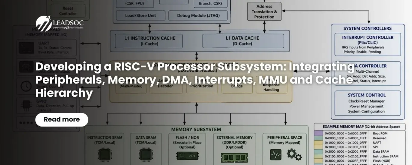
A simplified subsystem can be viewed as: RISC-V Core → Bus/Interconnect → Memory and Peripheral Address Space. Connected to the interconnect are memories such as Boot ROM, Instruction SRAM, and Data SRAM; non-volatile storage such as Flash; communication peripherals such as UART and SPI; and system-control blocks such as the DMA and interrupt controllers.
The interconnect performs address decoding and routes each transaction to the appropriate slave peripherals. In an advanced architecture, the interconnect may also incorporate arbitration, buffering, protocol conversion, access protection, quality-of-service mechanisms, and clock-domain crossing. This separation between the processor core and the SoC infrastructure is one of the important advantages of the RISC-V ecosystem — different RISC-V cores can be combined with different memory systems and peripheral configurations depending on the target application.
Memory-Mapped I/O
Memory-Mapped I/O (MMIO) is one of the fundamental concepts in processor-based SoC design. With MMIO, peripherals are assigned addresses within the processor's address space, and the processor accesses peripheral registers using normal load and store instructions, just as it accesses memory.
An illustrative address map is shown below. An actual SoC address map is defined by the architecture and system requirements.
| Address Range | Resource |
|---|---|
| 0x0000_0000 – 0x0000_0FFF | Boot ROM |
| 0x1000_0000 – 0x1000_0FFF | UART |
| 0x1000_1000 – 0x1000_1FFF | SPI |
| 0x2000_0000 – 0x2000_FFFF | Data SRAM |
| 0x2100_0000 – 0x2100_FFFF | Instruction SRAM |
| 0x3000_0000 – 0x30FF_FFFF | Flash |
| 0x4000_0000 – 0x4000_0FFF | DMA Controller |
| 0x4000_1000 – 0x4000_1FFF | Interrupt Controller |
Suppose the UART transmit register is located at 0x1000_0000. A processor writing to this address causes the UART hardware to transmit the given byte. From the software perspective, it appears as a memory write; from the hardware perspective, the interconnect recognizes the address as belonging to the UART and routes the transaction to the UART register interface. This approach provides a unified programming model — instead of requiring special processor instructions for every peripheral, software can access control and status registers through standard load/store operations.
Designing the Peripheral Interconnect
The interconnect is the central communication fabric connecting the RISC-V processor to memories and peripherals. For a small microcontroller-class subsystem, a relatively simple bus architecture may be sufficient, with the processor acting as the primary bus master while UART, SPI, SRAM, and other blocks act as slaves.
As the system becomes more sophisticated, there may be multiple masters — the RISC-V processor, DMA controller, debug module, and potentially accelerators may all need access to memory. In such systems, the interconnect requires arbitration, so the architecture becomes: Masters (Transfer initiators) → Arbitration/Interconnect → Address Decoder → Slaves (Data Receivers). The processor generates an address, read/write indication, and data; the address decoder determines the destination, routing the request to the SRAM controller, UART register interface, or Flash controller as appropriate. This architecture also provides a natural point for implementing access permissions, transaction ordering, error reporting, and performance monitoring.
Integrating the UART Peripheral Core
UART is typically one of the simplest peripherals to integrate and is extremely useful during SoC development. It usually has a set of memory-mapped registers such as transmit data, receive data, status, baud-rate configuration, and control registers. Software configures the UART by writing to its control registers and transmits data by writing to the transmit register. The UART can also generate interrupts — for example, when a character is received, prompting the processor to execute an interrupt service routine to read the received data. This makes UART useful both as a communication interface and as a debug and diagnostic mechanism during silicon bring-up.
Integrating SPI and External Flash
SPI is a serial interface for connecting external devices such as sensors, EEPROMs, Flash memories, and other controllers. When external Flash is connected through SPI, the processor may initially communicate with it through SPI controller registers, while an advanced SoC may have a dedicated Flash controller supporting memory-mapped or execute-in-place operation.
This distinction is important. In a simple system, software explicitly commands the SPI controller to read Flash data. In an execute-in-place architecture, instructions stored in Flash can potentially be fetched through a memory-mapped Flash interface, reducing the need to copy the entire application into SRAM before execution. Because Flash typically has higher access latency than SRAM, a cache can become particularly useful when executing code or reading frequently accessed data from Flash.
Boot ROM: Where Processor Execution Begins
The Boot ROM is a small non-volatile memory integrated into the SoC that contains the initial code executed after reset. When the processor comes out of reset, its program counter is configured to a predefined reset address that normally maps to the Boot ROM. The Boot ROM performs required initialization tasks such as configuring clocks, checking system status, initializing memory, determining the boot source, and loading or transferring control to the next stage of software.
In security-oriented SoCs, the Boot ROM can also form the root of trust, authenticating the next software stage before execution and establishing a secure boot chain. The Boot ROM therefore has a special architectural position: it is not simply another memory block, but the starting point of the processor's software execution environment.
Instruction SRAM and Data SRAM
Instruction SRAM and Data SRAM are often used to provide deterministic, low-latency memory close to the processor. Instruction SRAM stores executable instructions, while Data SRAM stores variables, stacks, buffers, and other runtime data.
Although both may physically use similar SRAM technology, separating instruction and data paths can provide architectural advantages — a processor can potentially fetch an instruction while simultaneously accessing data, particularly when the core implements separate instruction and data interfaces. This leads naturally toward Harvard or modified-Harvard architectures. For embedded real-time systems, SRAM is particularly attractive because its access latency is predictable, which matters in applications such as automotive controllers, industrial control, and sensor-processing systems where deterministic response can be more important than maximum average performance.
DMA Controller: Moving Data Without Occupying the CPU
As the amount of data handled by peripherals increases, using the processor to copy every byte becomes inefficient. This is where the Direct Memory Access (DMA) controller becomes important. The DMA controller acts as another bus master; software configures it by writing source address, destination address, transfer size, and control information into DMA registers, and once started, the DMA can move data directly between peripherals and memory.
For example, SPI → DMA → Data SRAM can transfer a large sensor data buffer without requiring the RISC-V processor to execute a load and store instruction for every data element. After completing the transfer, the DMA can generate an interrupt, and the processor then processes the completed buffer. This architecture significantly reduces CPU overhead and allows computation and data movement to proceed concurrently.
Interrupt Controller: Managing Asynchronous Events
Processors cannot continuously poll every peripheral to determine whether an event has occurred. An interrupt mechanism allows hardware to notify the processor when attention is required. UART, SPI, DMA, timers, and other peripherals can generate interrupt requests, which are collected and managed by the interrupt controller. The interrupt controller determines which interrupt should be presented to the RISC-V core and may provide prioritization and masking mechanisms.
A typical sequence is: Peripheral Event → Interrupt Request → Interrupt Controller → RISC-V Core → Interrupt Service Routine. For example, when a DMA transfer completes, the DMA controller asserts an interrupt, the interrupt controller forwards the event to the processor, and the processor saves the necessary execution state, enters the interrupt handler, checks the DMA status, and processes the newly available data. The interrupt architecture becomes increasingly important as the number of peripherals and processing tasks grows.
Complete Memory Map
Once all these blocks are integrated, the SoC architect must create a coherent address map. The memory map defines which physical address corresponds to which resource, and should consider the address width of the processor, memory capacity, peripheral requirements, future expansion, security regions, and operating-system requirements.
A well-designed memory map also simplifies software development. A typical embedded system might conceptually contain: Boot Region → Code/Flash Region → SRAM Region → Peripheral Region → DMA/Interrupt/System-Control Region. The actual address assignments should be designed according to the SoC architecture rather than simply assigning addresses sequentially, and address decoding must also ensure that an invalid address produces a well-defined bus error rather than an undefined system response.
Extending the Architecture with an MMU
A simple embedded RISC-V system can operate using physical addresses directly. As the processor becomes capable of supporting sophisticated operating systems, however, virtual memory becomes important — this is where the Memory Management Unit (MMU) is introduced. The MMU translates virtual addresses generated by software into physical addresses used to access the SoC memory system.
The basic path becomes: RISC-V Core → Virtual Address → MMU → Physical Address → Cache/Interconnect → Memory or Peripheral. The MMU provides address translation as well as memory protection mechanisms — different software processes can operate in separate virtual address spaces, while the operating system controls access to physical memory. For RISC-V systems implementing virtual memory, address translation is defined by the selected RISC-V privileged architecture scheme, and the MMU works with page tables maintained by software, typically under operating-system control. The introduction of an MMU therefore changes the architecture significantly, since the processor no longer necessarily sees the physical memory map directly.
MMU and Memory-Mapped Peripherals
A common architectural question is whether peripherals are also subject to virtual address translation. In a virtual-memory system, software can access a virtual address that maps to a physical peripheral address, and page-table attributes can define the region as appropriate for device access rather than normal cacheable memory. This distinction is critical — a UART register cannot generally be treated like ordinary cacheable SRAM. If a processor writes to a UART transmit register, the write must reach the peripheral rather than remaining indefinitely in a cache.
Consequently, memory attributes become an important part of MMU and cache architecture. The SoC designer must clearly distinguish between Normal Memory, which is cacheable and potentially speculative and buffered, and Device Memory, which requires controlled access with appropriate ordering and side-effect semantics. This is one of the areas where processor architecture, MMU design, cache design, and software architecture must work together.
Introduction to Cache Memory
As processor frequency increases, the processor can execute instructions much faster than external or even on-chip memory can supply data. Cache memory reduces this performance gap. A cache is a small, fast memory that stores recently accessed instructions or data. When the processor requests an address, the cache checks whether the required information is already available — if it is present, the processor receives the data quickly, a cache hit; if not, the system accesses the next level of memory hierarchy, a cache miss.
The fundamental principle is based on locality. Programs tend to repeatedly access recently used data and instructions, known as temporal locality, and access data located near recently accessed addresses, known as spatial locality.
Instruction Cache and Data Cache
A RISC-V processor subsystem may implement separate Instruction and Data caches. The Instruction Cache (I-Cache) stores recently fetched instructions, reducing instruction-fetch latency, while the Data Cache (D-Cache) stores frequently accessed data, reducing the number of accesses to slower memory.
The resulting processor architecture may look like: RISC-V Core → I-Cache / D-Cache → Memory System / Interconnect → SRAM / Flash / External Memory. This is particularly valuable when the processor executes software from relatively slow memory such as Flash.
A Memory Hierarchy
A modern processor subsystem rarely relies on a single memory type. Instead, it uses a hierarchy based on speed, capacity, and cost: CPU Registers → L1 Cache → L2 Cache → Local SRAM → External/Shared Memory → Flash/Storage.
Registers are extremely fast but limited in capacity. L1 cache is larger but slightly slower. L2 cache provides greater capacity with additional latency. SRAM provides substantial local storage but is slower than cache. External DRAM provides much greater capacity but introduces additional latency. Flash provides non-volatile storage but is substantially slower for random accesses. The architecture therefore balances performance, capacity, area, power, and cost. For a small embedded RISC-V SoC, registers, SRAM, and perhaps a small cache may be sufficient; for an application-class processor, multi-level caches and external DRAM become important.
Putting the Architecture Together
A complete RISC-V processor subsystem can therefore evolve from a relatively simple embedded architecture into a sophisticated application processor. A representative architecture flows from the RISC-V Core through the MMU, L1 Instruction Cache and L1 Data Cache, an L2 Cache/Memory System, and a System Interconnect, which then branches out to Instruction SRAM, Data SRAM, and Flash/DRAM, alongside peripherals such as UART, SPI, DMA, Interrupt Controller, Timers, and other peripherals.
Boot ROM provides the initial execution environment, the DMA controller enables efficient movement of data, and the interrupt controller manages asynchronous system events. The organization depends heavily on the application. A microcontroller-oriented RISC-V SoC may eliminate the MMU and large caches in favor of deterministic SRAM. An automotive or industrial processor may use tightly coupled memories alongside caches to achieve predictable real-time performance. An application processor running Linux may require an MMU, multiple cache levels, external DRAM, and sophisticated interrupt and memory-management infrastructure.
Verification of the RISC-V Subsystem
Integrating the individual IP blocks is only the beginning — the complete subsystem must be verified at multiple levels. At the block level, UART, SPI, DMA, SRAM, Flash controller, and interrupt controller are verified independently. At the subsystem level, the interaction between the processor, interconnect, and peripherals must be verified.
Important scenarios include processor boot from Boot ROM, instruction execution from SRAM or Flash, peripheral register accesses, DMA transfers, interrupt generation, simultaneous processor and DMA memory accesses, invalid address accesses, and reset/recovery behavior. When an MMU and caches are introduced, verification becomes significantly more complex — address translation, page-table handling, access permissions, cache hits and misses, memory attributes, exceptions, and coherency behavior must all be considered.
Software-driven verification becomes particularly valuable here. Firmware can exercise realistic sequences such as: Boot ROM → Flash initialization → Program loading → SRAM initialization → UART configuration → SPI data acquisition → DMA transfer → Interrupt → Data processing. This provides a much more meaningful validation of the integrated subsystem than testing each IP independently.
Design Considerations for a Production SoC
A production-quality RISC-V subsystem requires architectural decisions beyond simply connecting IP blocks. Clock and reset architecture must be defined carefully, particularly when peripherals operate at different frequencies. Low-power modes may require selective clock and power gating. Security requirements may require secure and non-secure address regions, access control, and secure boot.
The bus architecture must also accommodate bandwidth requirements — a DMA controller transferring large amounts of data can compete with the processor for memory bandwidth. Cache architecture must be selected according to workload, and SRAM size must be balanced against silicon area and power. For automotive and other safety-critical applications, fault handling, error detection, memory protection, and deterministic behavior become additional design considerations. These decisions demonstrate an important principle in SoC design: processor integration is a system architecture problem, not simply an RTL integration exercise.
Role of SoC Design Expertise
A RISC-V core may be available as an IP block, and UART, SPI, DMA, SRAM, and interrupt-controller IPs may also be reusable. The real engineering challenge is integrating these components into a coherent system. The SoC designer must understand processor architecture, bus protocols, memory systems, address translation, cache behavior, interrupt mechanisms, firmware requirements, clock/reset design, and verification methodology.
The architecture must be designed backward from the intended application. For a sensor-processing SoC, deterministic SRAM access and DMA may be more important than a large cache hierarchy. For an automotive application processor, memory protection, safety mechanisms, and predictable interrupt response may dominate. For a Linux-capable RISC-V processor, the MMU, cache hierarchy, external memory interface, and interrupt architecture become fundamental.
Conclusion
Integrating a RISC-V processor with UART, SPI, Flash, Instruction SRAM, Data SRAM, Boot ROM, DMA, and an interrupt controller creates the foundation of a functional SoC processor subsystem. Memory-mapped I/O provides a unified mechanism for the processor to communicate with peripherals, while the system interconnect provides the address decoding and transaction routing required to connect the individual IP blocks.
As system requirements grow, the architecture can be extended with an MMU to support virtual memory and protection, and with caches to bridge the performance gap between the processor and the memory system. The resulting memory hierarchy allows the designer to balance performance, capacity, power, and silicon area.
For SoC designers, the key is to view the RISC-V core as the computational center of a complete system comprising processing, memory, communication, data movement, interrupt management, protection, and software execution infrastructure. This system-level understanding is what turns reusable RISC-V and peripheral IP into a production-ready SoC.
Stay Connected with LeadSOC
LeadSOC brings together expertise across RISC-V processor integration, RTL design, verification, memory subsystem design, SoC interconnect, peripheral integration, and system-level validation. Follow LeadSOC for more practical insights into building advanced processor-based SoCs.
Subscribe Now