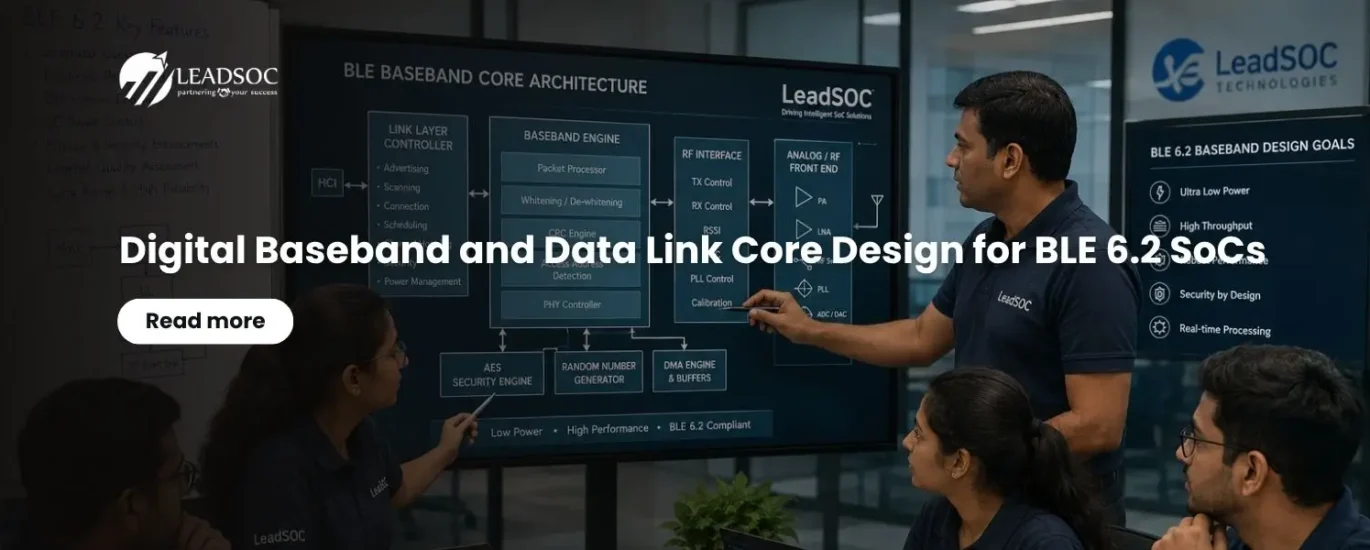
Digital Baseband and Data Link Core Design for BLE 6.2 SoCs
Engineering Insights · LeadSoC Technologies
Bluetooth® Low Energy (BLE) has evolved from a simple wireless connectivity protocol into the communication backbone for IoT devices, industrial automation, smart healthcare, wearables, smart homes, automotive systems, and intelligent edge computing. The BLE 6.2 specification further enhances reliability, security, positioning accuracy, coexistence, and power efficiency, making it an ideal wireless technology for next-generation connected products.
While the Analog/RF Front End determines the radio performance of a BLE device, the Digital Baseband and Data Link cores determine how efficiently information is transmitted, protected, synchronized, and managed. A high-performance BLE SoC requires these digital blocks to be designed together with the Analog/RF subsystem to achieve protocol compliance, optimum power consumption, and reliable wireless communication.
Digital Baseband
The Digital Baseband is the processing engine between the Link Layer and the Analog/RF Front End. It converts packet data generated by the data link and higher protocol layers into precisely timed digital waveforms transmitted by the RF subsystem, and ensures that incoming packets are correctly received and forwarded to the upper layers.
The baseband performs several critical operations, including packet framing, address insertion and detection, CRC generation and verification, data whitening and de-whitening, packet synchronization, timing generation, channel selection, RSSI acquisition, PHY control, automatic acknowledgements, and power management coordination. Since BLE communication operates with timing accuracy in the microsecond range, these functions are typically implemented as dedicated hardware accelerators to ensure deterministic performance.
Data Link Layer (Link Layer Controller)
The Data Link Layer, commonly referred to as the Link Layer Controller (LLC), manages every communication event throughout the lifetime of a BLE connection. It controls advertising, scanning, connection setup, packet scheduling, adaptive frequency hopping, encryption, connection parameter updates, and low-power transitions.
In BLE 6.2, the Link Layer also supports advanced features such as improved coexistence mechanisms, periodic advertising, isochronous communication, and simultaneous multi-role operation. Rather than simply forwarding packets, the Link Layer continuously coordinates transmission and reception events with the RF subsystem while optimizing energy consumption and maintaining protocol timing requirements.
Architecture of a BLE 6.2 Digital SoC
A modern BLE 6.2 digital subsystem consists of several tightly integrated hardware engines working together as a real-time communication processor. The architecture typically includes the Host Controller Interface (HCI), Link Layer Controller, Digital Baseband Engine, Packet Processing Engine, AES Security Engine, Random Number Generator, Channel Selection Engine, DMA Controller, Scheduler, Power Management Controller, Clock Management Unit, Sleep Controller, Register Configuration Interface, Interrupt Controller, and a dedicated RF Control Interface.
These hardware blocks operate concurrently using pipelined architectures to process BLE packets with minimal latency while maintaining extremely low power consumption. The modular organization also enables scalability for future protocol enhancements and simplifies integration into larger IoT and automotive SoCs.
| Hardware Block | Primary Role |
|---|---|
| Host Controller Interface (HCI) | Standardized command/event boundary between Host and Controller |
| Link Layer Controller | Manages connections, scheduling, hopping, and encryption |
| Digital Baseband Engine | Converts packets to/from precisely timed digital waveforms |
| Packet Processing Engine | Real-time packet framing, CRC, and payload handling |
| AES Security Engine | Encryption, authentication, and privacy address generation |
| Channel Selection Engine | Adaptive frequency hopping and channel map management |
| DMA Controller | Autonomous packet transfer between memory and buffers |
| Hardware Scheduler | Precision timing for advertising, scanning, and sleep events |
| Power Management Controller | Clock/power gating and low-power state coordination |
| RF Control Interface | Nanosecond-level synchronization with the Analog/RF front end |
Digital Packet Processing Pipeline
BLE packet transmission and reception follow a synchronized processing pipeline. During transmission, application data is encapsulated into Link Layer packets, followed by header generation, CRC calculation, data whitening, buffering, PHY formatting, and finally delivery to the Analog/RF transmitter. During reception, the reverse sequence is executed, where incoming radio signals are synchronized, decoded, checked for CRC integrity, de-whitened, parsed, and delivered to the Link Layer.
Each stage of this pipeline is optimized for throughput and implemented using dedicated hardware state machines. Pipelined processing significantly reduces latency while allowing the processor subsystem to remain in low-power states whenever possible.
Packet Processing Engine
The Packet Processing Engine performs all real-time packet manipulation required by the BLE protocol. It identifies packet boundaries, detects the Access Address, extracts packet headers, calculates and verifies CRC values, processes payload data, determines packet length, filters invalid packets, and automatically generates acknowledgements whenever required.
Modern BLE implementations rely on highly parallel packet processing architectures that execute multiple operations simultaneously. This reduces packet latency and enables support for higher throughput while minimizing overall energy consumption.
Adaptive Channel Selection
Reliable wireless communication depends heavily on intelligent channel management. BLE employs Adaptive Frequency Hopping to avoid interference from Wi-Fi networks and other devices operating within the crowded 2.4 GHz ISM band.
The Channel Selection Engine continuously evaluates channel quality, generates hopping sequences using Channel Selection Algorithm #2, updates channel maps, removes noisy frequencies, and remaps communication channels to maintain reliable connectivity. BLE 6.2 further enhances coexistence capabilities, making channel management one of the most critical digital functions within the SoC.
Hardware Scheduler
The hardware scheduler acts as the timing controller of the BLE subsystem. It determines the precise instant when advertising events, scanning windows, connection intervals, periodic synchronization, calibration routines, and sleep transitions occur.
By implementing scheduling entirely in hardware, processor wakeups are minimized, significantly reducing power consumption while ensuring compliance with strict BLE timing specifications. This autonomous scheduling capability is particularly valuable for battery-powered IoT devices that spend most of their operational lifetime in sleep mode.
Hardware Security Engine
Security remains one of the most important aspects of BLE communication. BLE 6.2 continues to utilize AES-128 encryption together with authentication and privacy mechanisms to protect wireless communication.
Dedicated hardware accelerators perform encryption, CCM authentication, random number generation, secure pairing support, privacy address generation, and cryptographic key management. Implementing these functions in hardware not only improves performance but also reduces processor workload and minimizes energy consumption during secure communication sessions.
DMA and Memory Architecture
Efficient movement of packet data is essential for maintaining communication throughput. The DMA engine transfers packet data between memory and packet buffers without processor intervention, allowing the CPU to remain in low-power states.
The memory subsystem typically supports multiple transmit and receive buffers, scatter-gather transfers, circular queue management, automatic descriptor handling, and interrupt generation. These features collectively improve communication efficiency while reducing overall system latency and processor utilization.
Digital Interface to the Analog/RF Front End
The Digital Baseband and Analog/RF Front End must operate as a single coordinated subsystem. Continuous communication between digital logic and RF hardware ensures that packet timing, modulation, frequency synthesis, receiver gain, and calibration occur with extremely high precision.
The digital subsystem controls transmitter and receiver enable signals, power amplifier activation, low-noise amplifier control, frequency selection, automatic gain control, RSSI measurement, PLL synchronization, ADC/DAC timing, packet synchronization, RF calibration, and production test modes. Since BLE communication depends on deterministic timing, these interfaces are designed with nanosecond-level synchronization accuracy.
Analog/RF Front End
Although the Digital Baseband performs protocol processing, wireless performance ultimately depends on the capabilities of the Analog/RF Front End. The RF architecture must deliver excellent receiver sensitivity, transmitter spectral purity, fast channel switching, low phase noise, low power consumption, and robust coexistence with other wireless technologies operating within the 2.4 GHz band.
A BLE 6.2 RF Front End typically integrates a Low Noise Amplifier, Power Amplifier, RF switch, fractional-N PLL frequency synthesizer, quadrature mixers, variable gain amplifiers, automatic gain control circuitry, high-performance ADCs and DACs, calibration engines, crystal oscillator interfaces, and digital control logic. The RF subsystem must also support rapid wake-up from sleep, stable frequency accuracy, temperature compensation, and continuous calibration to meet the stringent performance requirements of modern wireless applications.
Digital Compensation of RF Impairments
Modern BLE SoCs increasingly rely on digital signal processing to compensate for analog imperfections. Rather than attempting to eliminate every RF impairment through analog circuit design alone, many corrections are performed digitally after signal reception.
The Digital Baseband continuously compensates for DC offset, IQ imbalance, carrier frequency offset, timing errors, automatic gain adjustments, RSSI calibration, packet quality estimation, adaptive transmit power control, and temperature-induced RF variations. This digital calibration approach simplifies analog design, improves manufacturing yield, and enables consistent performance across process, voltage, and temperature variations.
Low-Power Design Methodology
Power efficiency is a primary design objective for BLE devices, many of which operate for several years from a single battery. The Digital Baseband therefore incorporates extensive power management techniques, including clock gating, power gating, memory retention, dynamic voltage scaling support, autonomous wake-up controllers, hardware event scheduling, and low-leakage design methodologies.
The Analog/RF Front End complements these techniques through fast PLL locking, rapid calibration, low startup current, efficient transmit power control, and minimized active radio time. Together, these optimizations enable ultra-low average power consumption without compromising communication reliability.
Automotive Safety and Security Considerations
Automotive BLE implementations demand significantly higher levels of reliability than consumer devices. Beyond protocol compliance, the digital architecture must incorporate functional safety, diagnostics, and cybersecurity features suitable for safety-critical applications.
The digital subsystem typically includes ECC-protected memories, CRC-protected internal buses, clock monitoring, Built-In Self-Test (BIST), secure boot support, Hardware Root of Trust, authenticated debugging, fault injection detection, safety diagnostics, and error reporting mechanisms. The Analog/RF Front End similarly provides production test support, transmitter monitoring, receiver sensitivity diagnostics, calibration verification, and continuous health monitoring to satisfy automotive quality and reliability requirements.
Verification Strategy
Verification of a BLE 6.2 SoC extends well beyond functional RTL simulation. Successful product development requires comprehensive verification across digital, analog, RF, firmware, and system levels.
A complete verification methodology includes UVM-based protocol verification, formal verification of critical control logic, mixed-signal co-simulation, RF behavioral modeling, hardware/software co-verification, FPGA prototyping, emulation, interoperability testing, compliance verification, and post-silicon validation. Verification environments must accurately model RF impairments, timing variations, coexistence scenarios, low-power transitions, and protocol corner cases to ensure first-silicon success.
Conclusion
The Digital Baseband and Data Link cores serve as the intelligence behind every BLE 6.2 SoC, executing complex packet processing, scheduling, security, and power management functions with deterministic real-time performance. Their success, however, depends on seamless integration with an Analog/RF Front End capable of delivering exceptional wireless performance through high sensitivity, spectral purity, rapid channel switching, and adaptive calibration.
The future of BLE SoC development lies in holistic hardware-software-RF co-design, where digital intelligence and analog excellence work together to create highly integrated, low-power, and standards-compliant wireless solutions. Leveraging expertise in RISC-V processor integration, wireless protocol implementation, AMS verification, low-power SoC design, functional safety, and advanced physical implementation, LeadSoC has the complete capability to develop scalable BLE 6.2 solutions for IoT, industrial automation, healthcare, consumer electronics, and automotive applications.
LeadSoC's expertise across digital design, Analog/RF integration, mixed-signal verification, embedded software, and complete SoC implementation enables the delivery of robust BLE 6.2 platforms that address the demanding requirements of next-generation connected systems.
Build Your Next BLE 6.2 SoC
At LeadSoC Technologies, our engineering teams bring deep expertise in digital baseband, Link Layer, and RF co-design, helping customers ship robust, standards-compliant BLE SoCs from concept to silicon.
Subscribe to LeadSoC Blogs