SerDes Interface Design for
PCIe Gen5 and Gen6 SoCs
Modern high-performance SoCs are increasingly defined by the speed at which they transfer data, not merely the speed at which they compute it. At the heart of that transfer sits the Serializer/Deserializer — the SerDes subsystem — the critical technology enabling PCIe Gen5 and Gen6 communication across AI accelerators, cloud infrastructure, networking equipment, and advanced automotive platforms.
SerDes in PCIe SoCs
The SerDes PHY serves as the bridge between the digital PCIe controller and the physical transmission medium. Its primary function is to convert wide parallel data generated by the controller into high-speed serial streams for transmission across package traces, PCB channels, connectors, or cables. On the receive side, incoming serial data is recovered, equalized, deserialized, and reconstructed into parallel data for protocol processing.
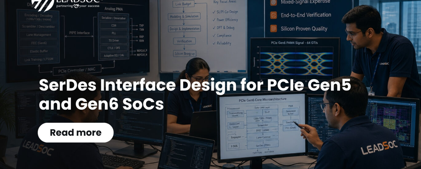
In modern PCIe implementations, the PHY is architecturally divided into two major domains: the Physical Coding Sublayer (PCS) and the Physical Medium Attachment (PMA). This partitioning allows protocol processing and high-speed analog signaling functions to be designed and optimized independently while maintaining seamless interoperability.
The Digital PCS: Protocol Intelligence at High Speed
The PCS forms the digital intelligence layer of the PCIe PHY. It ensures protocol compliance and maintains data integrity throughout transmission and reception — performing data encoding, scrambling, block alignment, ordered-set generation and detection, lane management, elastic buffering, and support for link training sequences.
Communication between the PCIe controller and PHY is typically implemented using the industry-standard PIPE interface. Signals such as TxData, RxData, PhyStatus, PowerDown, and Rate provide the operational framework for establishing and maintaining a PCIe link.
As PCIe evolves from Gen5 to Gen6, the digital complexity of the PCS increases significantly. The introduction of PAM4 signaling, Forward Error Correction (FEC), and flit-based transport requires sophisticated processing pipelines and tighter interaction between protocol logic and physical-layer adaptation mechanisms.
The Analog PMA: Signal Integrity at Multi-Gigahertz Speeds
While the PCS ensures protocol correctness, the PMA is responsible for communicating data reliably across increasingly challenging electrical channels. The PMA contains the serializer, deserializer, high-speed phase-locked loops, clock and data recovery circuits, transmit drivers, receiver equalization blocks, and adaptive calibration engines.
At data rates reaching 64 GT/s, signal integrity challenges become dominant. Channel attenuation, reflections, crosstalk, jitter, and process variations can significantly impact link performance. The PMA must continuously compensate for these impairments while maintaining low Bit Error Rates and robust link operation across all operating conditions.
| Specification | PCIe Gen5 | PCIe Gen6 |
|---|---|---|
| Data Rate | 32 GT/s | 64 GT/s |
| Signaling | NRZ (2 levels) | PAM4 (4 levels) |
| Forward Error Correction | Optional | Mandatory |
| Transport Mode | Packet-based | Flit-based |
| Voltage Margin | Higher | Reduced (4-level eye) |
| Primary Design Challenge | Channel loss, jitter sensitivity | Noise margin, FEC latency, distortion |
PCIe Gen5: Scaling Performance with NRZ Signaling
PCIe Gen5 doubled the bandwidth of its predecessor while continuing to use Non-Return-to-Zero (NRZ) signaling. Although the signaling methodology remained unchanged, the increased data rate introduced significant design challenges — channel losses became more severe, timing margins narrowed, and receiver sensitivity to jitter increased substantially.
Achieving compliance at 32 GT/s requires carefully optimized transmitter equalization, advanced receiver adaptation techniques, and accurate modeling of package and board-level effects. Power consumption also becomes a critical concern, particularly in large multi-lane implementations used in data center and AI applications.
These challenges have transformed SerDes development from a primarily circuit-level problem into a multidisciplinary optimization exercise spanning architecture, signal integrity, package design, and verification.
PCIe Gen6: The PAM4 Transition and Architectural Redefinition
PCIe Gen6 represents one of the most significant transitions in the history of the standard. Rather than simply increasing frequency, Gen6 introduces Pulse Amplitude Modulation with four signal levels (PAM4), effectively doubling throughput without doubling channel bandwidth requirements.
While PAM4 enables higher performance, it also reduces voltage margins significantly compared to NRZ. The receiver must now distinguish between four voltage levels instead of two — making links far more susceptible to noise, distortion, and channel impairments. To maintain acceptable reliability, PCIe Gen6 makes Forward Error Correction (FEC) mandatory.
The addition of FEC introduces new architectural considerations around latency, throughput, error monitoring, and verification — producing a PHY architecture that combines sophisticated digital processing with highly adaptive analog circuitry to achieve reliable operation at unprecedented data rates.
Adaptive Equalization and Link Optimization
As channel losses continue to increase, adaptive equalization has become a cornerstone of modern SerDes design. The receiver continuously monitors incoming signals and dynamically adjusts equalization parameters to maximize eye opening and minimize error rates.
Techniques such as Continuous Time Linear Equalization (CTLE), Decision Feedback Equalization (DFE), and adaptive clock recovery enable the receiver to compensate for channel impairments caused by package routing, PCB traces, connectors, and environmental variations. In PCIe Gen6, these adaptive mechanisms operate continuously throughout link operation, responding dynamically to changes in process, voltage, and temperature.
The Growing Importance of Digital-Analog Co-Design
The boundary between digital and analog design disciplines is becoming increasingly blurred in advanced SerDes architectures. Digital algorithms now influence equalization behavior, adaptation strategies, and error correction mechanisms, while analog performance directly impacts protocol margins and system reliability.
Successful PCIe Gen5 and Gen6 implementations require close collaboration between digital architects, analog designers, signal integrity specialists, and verification teams. Link-budget analysis, channel modeling, equalization strategy development, and silicon characterization must be approached as an integrated engineering effort — not isolated activities. This digital-analog co-design methodology has become a key enabler for first-pass silicon success in high-speed interface development.
First-pass silicon success in high-speed interface development depends on treating link budget, channel modeling, and equalization strategy as a single integrated effort — not a handoff between teams.
Verification Challenges in Modern SerDes Designs
Verification of PCIe SerDes subsystems has grown significantly more complex with Gen5 and Gen6 technologies. Traditional digital verification techniques must now be complemented by mixed-signal verification methodologies capable of capturing both protocol correctness and analog behavior simultaneously.
Verification environments typically combine SystemVerilog, UVM, behavioral SerDes models, and analog abstraction techniques to validate link training, equalization convergence, error recovery, compliance patterns, and interoperability scenarios. Extensive modeling of channel characteristics and jitter behavior is required to ensure robust operation across all supported configurations. As data rates increase, comprehensive verification becomes ever more critical to achieving compliance and reducing costly silicon re-spins.
Conclusion
PCIe Gen5 and Gen6 SerDes interfaces represent the convergence of advanced digital architecture, precision analog design, signal integrity engineering, and sophisticated verification methodologies. The transition from 32 GT/s NRZ signaling to 64 GT/s PAM4 operation has fundamentally reshaped PHY development — requiring unprecedented levels of innovation and interdisciplinary collaboration.
As AI infrastructure, cloud computing platforms, networking systems, and high-performance computing applications continue to demand higher bandwidth, SerDes technology will remain a foundational building block of next-generation SoCs.
Build PCIe Gen5 & Gen6 Solutions with LeadSoC
Our engineering teams bring deep expertise in high-speed interface architecture, mixed-signal verification, protocol compliance, and SoC integration — enabling customers to successfully develop and deploy PCIe Gen5 and Gen6 solutions from concept to silicon.
Subscribe to LeadSoC Blog
Written by
Murshad KP
Digital Marketing Manager — Google Ads, Meta, SEO for B2B Tech, Semiconductor, Healthcare & D2C brands.
Connect on LinkedIn