Static Timing Analysis Fundamentals and the SDC File
VLSI Design · Timing Closure · Synopsys Design Constraints (SDC)
Introduction
A successful System-on-Chip (SoC) design must do more than implement the required logic. It must transfer data correctly between registers, communicate reliably with external devices, and operate within specified performance limits. Timing constraints provide the foundation for achieving these objectives.
They tell synthesis and implementation tools how quickly the design must operate, when input data is expected to arrive, when output data must be available, and how clocks relate to one another. Incomplete or unrealistic constraints can lead to poor optimization — or timing reports that look clean while important paths remain unchecked.
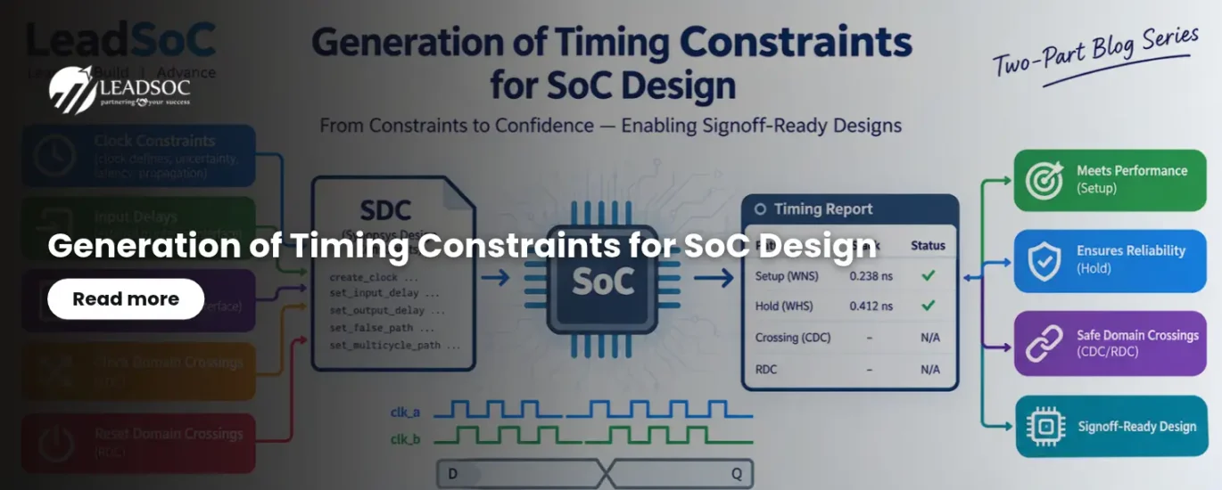
This is the first of a two-part LeadSoc blog series. Part 1 introduces Static Timing Analysis (STA), the Synopsys Design Constraints (SDC) format, and the process of defining clocks and interface timing. Part 2 will be published on the subsequent Monday and will cover timing-report interpretation, a practical two-clock analysis procedure, Clock Domain Crossing (CDC), and Reset Domain Crossing (RDC). Readers are encouraged to follow the second part next week to complete the flow from constraint generation to signoff checks.
1. What Is Static Timing Analysis?
Static Timing Analysis is a method of verifying circuit timing by examining signal propagation through the design. Unlike simulation, STA does not need a test vector for every possible functional condition. It uses circuit connectivity, cell delay models, interconnect estimates or extracted parasitics, clock definitions, and timing constraints to evaluate timing paths.
A typical register-to-register path begins at a launching register, passes through combinational logic, and ends at a capturing register. Data leaves the launching register after its clock-to-Q delay, propagates through logic and interconnect, and must reach the receiving register within the allowed timing window.
The key calculation compares data arrival time with data required time. The difference is called slack. Positive setup slack means data arrives before its deadline; negative setup slack indicates a violation. Hold analysis checks the opposite risk: data must not arrive too early after the capture edge.
| Term | Meaning |
|---|---|
| Clock period | Time between consecutive active edges of a clock. |
| Clock-to-Q delay | Delay from the active clock edge to a register output response. |
| Setup time | Time data must be stable before the receiving clock edge. |
| Hold time | Time data must remain stable after the receiving clock edge. |
| Data arrival time | Calculated time at which data reaches the endpoint. |
| Data required time | Latest or earliest permitted arrival, depending on the check. |
| Slack | Difference between required time and actual arrival time. |
| Clock skew | Difference in clock arrival times at launch and capture points. |
| Clock uncertainty | Timing margin for jitter, variation, and other clock effects. |
2. Setup and Hold: Two Different Checks
For a simplified same-clock setup path, the data path must fit within the clock period after accounting for clock-to-Q delay, combinational delay, setup time, and uncertainty. Clock latency and skew also affect the actual required time.
Setup violations commonly require reducing data-path delay, improving placement, resizing cells, reducing logic depth, or revisiting a valid architectural timing assumption. Hold violations commonly require increasing minimum path delay, for example by inserting delay cells or buffers. A repair for one check must not cause failure in the other.
3. The Relevance of Timing Constraints
Timing constraints describe the operating environment of the chip. Consider a processor subsystem receiving sensor data, processing it in one clock domain, and communicating with a peripheral in another. The design may contain register-to-register paths, input-to-register paths, register-to-output paths, and crossings between clock domains. Each path category needs an appropriate timing model.
An incorrect clock period can make the tool optimize for the wrong performance target. An incorrect input delay can underestimate the time already consumed outside the chip. An incorrect output delay can leave insufficient time for an external receiver. Constraints should therefore be derived from system specifications, interface timing diagrams, and the clock architecture — not copied blindly from an earlier project.
4. Timing Constraints in SDC File Format
SDC is a Tcl-based constraint format widely used by synthesis, timing analysis, and physical implementation tools. An SDC file is normally a text file with the .sdc extension. Commands define clocks, interface timing, electrical assumptions, and timing exceptions. The exact supported options can vary by tool and version.
create_clock -name SYS_CLK \
  -period 10.000 [get_ports sys_clk]
This command defines a clock named SYS_CLK with a 10 ns period on the top-level port sys_clk. Its frequency is 100 MHz. The get_ports command selects the design port. Other common object selectors include get_pins, get_cells, and get_clocks.
5. The Main Sections of an SDC File
Clock definitions: create_clock and create_generated_clock define primary and generated clocks, periods, waveforms, and relationships.
Interface timing: set_input_delay and set_output_delay model external data arrival and capture requirements.
Clock and signal characteristics: set_clock_uncertainty, set_clock_latency, set_input_transition, and set_load model timing margins and electrical conditions.
Timing exceptions: set_false_path, set_multicycle_path, set_max_delay, set_min_delay, and asynchronous clock-group declarations describe justified exceptions or special path requirements.
6. Defining Clocks and Their Characteristics
A clock definition specifies the period and, when needed, the active-edge waveform. For a 100 MHz clock with a 50% duty cycle:
create_clock -name SYS_CLK \
  -period 10.000 \
  -waveform {0.000 5.000} \
  [get_ports sys_clk]
For a 50 MHz peripheral clock:
create_clock -name PERIPH_CLK \
  -period 20.000 \
  -waveform {0.000 10.000} \
  [get_ports periph_clk]
If a clock is generated internally by a divider, phase-locked loop, or another clock-generation circuit, its actual relationship should be modeled. Where appropriate, use create_generated_clock instead of treating a related generated clock as an unrelated primary clock.
Clock uncertainty accounts for effects such as jitter, variation, and residual timing margin. Illustrative setup and hold uncertainty constraints are shown below. Values must come from the design's timing methodology.
set_clock_uncertainty -setup 0.200 [get_clocks SYS_CLK]
set_clock_uncertainty -hold  0.050 [get_clocks SYS_CLK]
Clock latency models the time for a clock to reach a point in the clock network. Before clock-tree synthesis, the flow may use ideal-clock assumptions or estimated latency. After clock-tree synthesis, actual or propagated clock delays are analyzed according to the implementation methodology. Avoid double-counting latency already modeled elsewhere.
7. Input Delays and Output Delays
7.1 Input Delay
Input delay is the arrival time of data at a chip input relative to a reference clock edge. Depending on the interface model, it can include external device clock-to-output delay, board propagation delay, and other components outside the chip.
Suppose an external sensor and board require up to 2 ns for data to reach the SoC input, relative to the selected reference edge. An illustrative constraint is:
set_input_delay -max 2.000 -clock SYS_CLK [get_ports sensor_data]
set_input_delay -min 0.500 -clock SYS_CLK [get_ports sensor_data]
Maximum input delay is used for setup analysis; minimum input delay is used for hold analysis. Values must be based on the interface specification. Use separate rise and fall values when the interface timing requires them.
7.2 Output Delay
Output delay represents external timing requirements relative to a specified clock edge. If a peripheral must capture output data 2 ns before its reference edge, an illustrative maximum output delay is:
set_output_delay -max 2.000 -clock PERIPH_CLK [get_ports result_data]
set_output_delay -min 0.500 -clock PERIPH_CLK [get_ports result_data]
The minimum output delay models the external hold requirement and interface timing relationship. It is not always positive; a valid value may be zero or negative depending on the external device, board delay, and clock skew. Input and output delays are relative timing constraints — not estimates of delay inside the chip.
8. Electrical Constraints: Input Transition and Output Load
Electrical assumptions influence cell delay and synthesis optimization. Input transition affects the delay of the first receiving cell. Output load affects the final stage's delay and drive-strength requirements.
set_input_transition 0.100 [get_ports sensor_data]
set_load              0.050 [get_ports result_data]
These example values represent a 100 ps input transition and a 0.050 pF output load, assuming consistent units. They are illustrative only; the actual values should reflect the target interface and library conventions.
9. Example: A Two-Clock SoC Constraint Skeleton
Consider a simple sensor-processing SoC with SYS_CLK at 100 MHz and PERIPH_CLK at 50 MHz. The following example brings together the main SDC sections. Port names and values must be adapted to the actual RTL and system timing specifications.
# Primary clocks
create_clock -name SYS_CLK -period 10.000 \
  -waveform {0.000 5.000} [get_ports sys_clk]
create_clock -name PERIPH_CLK -period 20.000 \
  -waveform {0.000 10.000} [get_ports periph_clk]

# Clock uncertainty (illustrative)
set_clock_uncertainty -setup 0.200 [get_clocks SYS_CLK]
set_clock_uncertainty -hold  0.050 [get_clocks SYS_CLK]
set_clock_uncertainty -setup 0.300 [get_clocks PERIPH_CLK]
set_clock_uncertainty -hold  0.080 [get_clocks PERIPH_CLK]

# Input timing
set_input_delay -max 2.000 -clock SYS_CLK [get_ports sensor_data]
set_input_delay -min 0.500 -clock SYS_CLK [get_ports sensor_data]

# Output timing
set_output_delay -max 2.000 -clock PERIPH_CLK [get_ports result_data]
set_output_delay -min 0.500 -clock PERIPH_CLK [get_ports result_data]

# Electrical assumptions
set_input_transition 0.100 [get_ports sensor_data]
set_load              0.050 [get_ports result_data]
This skeleton assumes that sensor_data is timed relative to SYS_CLK and result_data relative to PERIPH_CLK. That assumption is valid only if the real external interfaces use those reference clocks, or if their timing has been translated appropriately. A two-clock design needs an explicit review of the relationship between the clocks; different names alone do not prove that they are asynchronous.
Conclusion — Continue in Part 2 Next Monday
Timing constraints translate system requirements into a model that synthesis, implementation, and timing-analysis tools can use. Accurate clock definitions, realistic input and output delays, appropriate electrical assumptions, and carefully justified exceptions are essential for meaningful timing results.
Stay Connected with LeadSoc
Stay connected with LeadSoc for practical insights into VLSI design methodology, RTL development, synthesis, physical design, verification, and advanced SoC engineering.
Subscribe Now