Co-Verification of a RISC-V Processor Subsystem: From Bootcode to Peripheral Access
RISC-V Verification · Hardware/Software Co-Verification · SoC Bring-up
Introduction
Designing a processor subsystem is significantly more than integrating a CPU core with memories and peripherals. The real engineering challenge begins when all these components have to operate together as a coherent system.
A RISC-V processor subsystem may contain the processor core, Boot ROM, Instruction SRAM, Data SRAM, UART, SPI, Flash interface, DMA controller, interrupt controller, bus/interconnect, memory management unit, cache hierarchy, and other application-specific peripherals. Each block can be individually verified, yet the complete subsystem can still fail when software begins interacting with the hardware. This is where co-verification becomes essential.
Co-verification validates the interaction between hardware and software. Instead of treating the processor as another RTL block, the verification environment executes real or representative bootcode, initialization software, peripheral drivers, and application programs on the processor while simultaneously monitoring the hardware behavior. The objective is to answer a fundamental question: can the complete processor subsystem boot, initialize itself, access memory and peripherals correctly, handle interrupts and DMA transactions, and execute software as intended?
From Processor Integration to System Verification
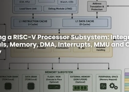
In the previous article on RISC-V processor subsystem integration, we discussed how a RISC-V processor can be extended into a complete processor subsystem by integrating Instruction SRAM, Data SRAM, Boot ROM, UART, SPI, Flash, DMA, and Interrupt Controller, along with Memory-Mapped I/O, the Memory Management Unit, and cache memory and hierarchy.
Once this architecture is available, the verification problem changes considerably. At the processor-core level, verification focuses on instructions, registers, exceptions, privilege modes, and architectural compliance. At the subsystem level, the focus expands to the complete transaction path: Software → Processor Core → Cache/MMU → Interconnect → Address Decoder → Memory/Peripheral → Response → Processor.
Every element in this path can influence the final software-visible behavior. For example, a UART may be perfectly verified independently, and the processor core may also be fully verified — but if the UART is mapped at an incorrect address, the software UART driver will fail. Similarly, if the bus transaction reaches the peripheral but the byte-enable, read/write control, or response timing is incorrect, the software may still observe a failure. Therefore, subsystem co-verification must validate functionality as observed by software, rather than only individual RTL interfaces.
The Role of Bootcode in Co-Verification
Bootcode is one of the most important components of processor subsystem verification. When the processor comes out of reset, it does not immediately execute an application — it starts execution from a predefined reset or Boot ROM address. The bootcode then performs the initial configuration required to bring the subsystem into a usable state.
A typical boot sequence may include: Reset release → Fetch instruction from Boot ROM → Stack initialization → Memory initialization → Peripheral initialization → Interrupt configuration → Flash access → Application image loading → Application execution. This sequence exercises a surprisingly large portion of the hardware, so a simple bootcode program can act as an early system-level integration test.
The first objective is to verify that the processor fetches the correct instruction from Boot ROM after reset, confirming the reset vector, instruction bus, address decoding, and Boot ROM connectivity. The next objective is to verify sequential instruction execution — the bootcode can perform arithmetic operations, branches, function calls, stack operations, and memory accesses, providing an early sanity check that the processor core and its surrounding instruction and data paths are functioning correctly. Bootcode also provides an excellent mechanism for validating hardware initialization registers: software writes configuration values into memory-mapped control registers and subsequently reads them back, confirming that the processor can correctly control the hardware.
Reset and Initialization Verification
Reset verification is the starting point of subsystem co-verification. The verification environment should exercise different reset scenarios and observe the processor and subsystem state after reset. Important checks include the processor program counter, register state, memory initialization status, peripheral reset states, interrupt controller state, and DMA controller state.
The bootcode should then establish a known system configuration — for example, initialization software may configure the UART baud rate, enable SPI, configure the DMA controller, initialize interrupt-controller registers, and establish memory regions. This provides an important distinction between hardware reset validation and software initialization validation. Hardware verification asks whether the hardware entered the correct reset state; co-verification additionally asks whether software can bring the hardware from the reset state to the required operational state. This distinction is fundamental in a real SoC.
Verifying the Memory Map
One of the most important responsibilities of subsystem co-verification is validating the system address map. Memory-mapped I/O allows software to access peripherals using normal load and store instructions — each peripheral is assigned an address range, and the interconnect or address-decoding logic routes processor transactions to the corresponding hardware block. The exact addresses depend on the subsystem architecture, but a conceptual memory map can be organized as shown below.
| Address Region | Function |
|---|---|
| Boot ROM | Processor bootcode |
| Instruction SRAM | Program storage |
| Data SRAM | Data and stack |
| Flash | Non-volatile storage |
| UART | Serial communication |
| SPI | Serial peripheral interface |
| DMA | Data movement control |
| Interrupt Controller | Interrupt configuration and status |
Co-verification must confirm that every address range produces the expected hardware response. A boot or diagnostic program can deliberately access each mapped region and perform read/write operations, while the verification environment simultaneously monitors the bus transaction and confirms that the correct slave is selected. This catches integration errors such as overlapping address ranges, incorrect address decoding, missing peripheral connections, and incorrect base addresses in software drivers.
Peripheral Access Through Software
Peripheral verification becomes particularly meaningful when the processor accesses the peripheral exactly as application software would. For UART verification, for example, software can write a character to the UART transmit register, and the co-verification environment can check the processor transaction, register update, and resulting serial output.
Similarly, an SPI test can configure the SPI controller through memory-mapped registers and initiate a transfer, while the verification environment monitors the SPI signals and compares the received data with the expected value. The same methodology can be extended to Flash: the processor may first configure the Flash controller, issue a read command, and then access Flash data through the appropriate memory or peripheral interface, validating not only the Flash controller but also the complete processor-to-Flash transaction path. This is an important advantage of co-verification — a single software test can simultaneously exercise multiple hardware blocks and their interconnections.
Instruction and Data Memory Verification
Instruction SRAM and Data SRAM should be verified from the processor's point of view. The bootcode can execute from Boot ROM initially and subsequently transfer execution to Instruction SRAM, verifying instruction fetches through the corresponding address path.
Data SRAM can be tested using software-generated patterns such as walking ones, walking zeros, alternating patterns, and pseudo-random data — the processor writes data into memory and subsequently reads it back for comparison, while the verification environment monitors these transactions and compares them against a reference model. This also provides an opportunity to validate interactions between Instruction SRAM, Data SRAM, and the cache hierarchy when caches are enabled.
Cache and MMU Co-Verification
Introducing caches and an MMU significantly increases subsystem verification complexity. The processor may generate a virtual address, which is translated by the MMU into a physical address; the cache hierarchy may then determine whether the requested data is available locally or whether a transaction must proceed to the memory subsystem. Consequently, a software load instruction can involve several hardware mechanisms before reaching SRAM or a peripheral.
Co-verification should therefore include tests for cache hits, cache misses, cache flushes, and invalidations where applicable. Memory attributes and regions used for memory-mapped peripherals must also be handled correctly — a critical requirement is ensuring that peripheral accesses are not incorrectly cached. For example, reading a UART status register must return the current hardware status rather than an old cached value, and writes to control registers must reach the peripheral rather than remaining in a cache. The MMU and cache therefore need to be verified not only for processor performance but also for correct software-visible memory behavior.
DMA Co-Verification
DMA introduces another level of complexity because data movement can occur independently of the processor. A typical DMA software test configures source address, destination address, transfer size, and control parameters through memory-mapped registers, and the processor then starts the DMA transfer.
The co-verification environment should check that the processor correctly configures the DMA controller, that the DMA controller generates the required bus transactions, that data is transferred correctly, that the processor can observe DMA completion, that the appropriate interrupt is generated when enabled, and that cache coherency requirements are correctly handled where applicable. DMA testing is particularly valuable because it exercises the interconnect, memory system, and interrupt mechanism together.
Interrupt Co-Verification
Interrupts form the bridge between hardware events and software response. A peripheral may generate an interrupt after completing an operation; the interrupt controller receives the request, applies its configuration, and signals the processor, which then executes the appropriate interrupt service routine.
A complete interrupt co-verification sequence therefore becomes: Peripheral event → Interrupt request → Interrupt Controller → Processor interrupt → Trap/exception handling → ISR execution → Peripheral status handling. This sequence must be validated end-to-end. UART receive interrupts, SPI completion interrupts, DMA completion interrupts, and timer interrupts are useful examples for subsystem testing. The test should verify not only that an interrupt reaches the processor, but also that the correct interrupt source is identified and that software can clear or acknowledge the interrupt correctly.
Boot-to-Application Testing
After individual initialization tests have passed, the next step is to execute a complete software flow. A representative sequence may be: Reset → Boot ROM → Initialize SRAM → Initialize UART → Configure SPI → Initialize DMA → Configure Interrupt Controller → Access Flash → Load application → Execute application.
This is one of the most valuable co-verification tests because it represents the actual operating sequence of the SoC. If the application executes successfully, a substantial portion of the processor subsystem has effectively been validated as an integrated system. For embedded applications, this can eventually evolve into execution of an RTOS, middleware, or application firmware.
Reference Models and Scoreboards
Although software execution provides a powerful stimulus mechanism, the verification environment still requires conventional verification infrastructure. Bus monitors can observe processor and peripheral transactions, protocol monitors can check interface correctness, and scoreboards can compare expected and actual transactions or data. A reference model can predict expected memory contents, peripheral responses, or DMA transfers.
Functional coverage can measure whether important subsystem scenarios have been exercised, including bootcode execution, all memory-map regions accessed, read and write accesses, peripheral initialization, UART transmission and reception, SPI transactions, Flash reads, DMA transfers, interrupt generation and servicing, cache hit and miss scenarios, exception handling, and reset and recovery scenarios. The objective is to move beyond simply asking whether the software test passed and determine how much of the subsystem functionality has actually been exercised.
Co-Verification Environment
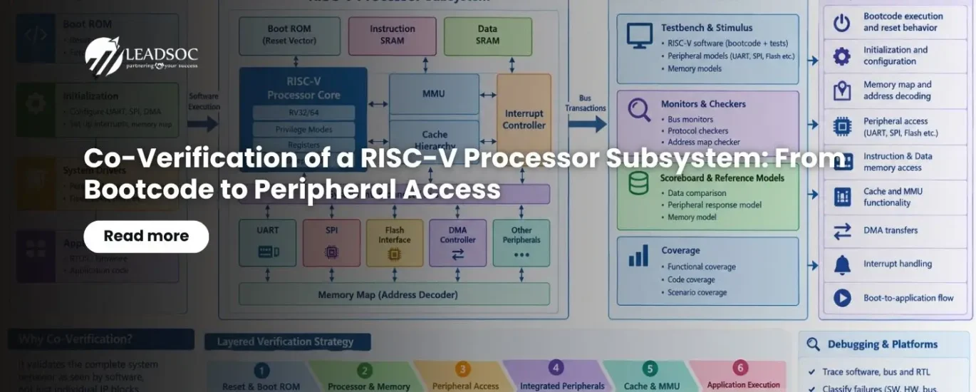
A typical processor-subsystem co-verification environment combines software and hardware verification components. At the top level, the RTL processor subsystem is connected to the verification environment. A RISC-V software image is compiled and loaded into Boot ROM, SRAM, or Flash models, and the processor executes this software during simulation while the verification environment observes internal and external interfaces.
The environment may contain a UART model, SPI model, Flash model, memory model, bus monitors, protocol checkers, scoreboards, and coverage collectors. The same software that eventually runs on silicon can therefore become a stimulus source during RTL simulation, creating a powerful bridge between hardware verification and firmware validation.
Debugging Co-Verification Failures
One of the major benefits of co-verification is that failures can be traced across hardware and software boundaries. Consider a simple software statement that writes to a UART register — if the expected output is not generated, debugging can proceed through the complete transaction path: Software instruction → Processor register state → Generated address → Bus transaction → Address decoder → UART register → UART state machine → Output signal.
A failure can therefore be classified as a software problem, processor problem, bus problem, address-map problem, peripheral-register problem, or peripheral-functional problem. Waveform analysis combined with processor trace and software logs provides a much more effective debugging methodology than testing hardware blocks independently.
From Simulation to FPGA and Emulation
Once the basic co-verification environment is established, the same software tests can progressively move toward faster platforms. RTL simulation provides detailed visibility and is useful for early debugging. FPGA prototyping enables much longer software execution and real peripheral interaction. Emulation can execute complex boot sequences and larger firmware workloads much faster than conventional RTL simulation, and post-silicon validation can eventually reuse many of the same software-based diagnostics.
This creates a continuous verification path: RTL Simulation → Emulation → FPGA Prototype → Silicon Bring-up. A well-designed co-verification strategy therefore provides value throughout the entire SoC development lifecycle.
Building a Layered Co-Verification Strategy
A robust methodology should not attempt to execute the complete application immediately. The recommended progression is to first validate reset and Boot ROM execution, followed by basic processor instruction execution and memory access. Peripheral address mapping can then be validated individually through software-driven register accesses.
Once individual peripherals are operational, integrated tests can combine UART, SPI, Flash, DMA, and interrupts. Cache and MMU functionality can subsequently be enabled and validated, and finally, complete bootcode and application workloads can be executed. This layered approach makes debugging significantly easier because each stage establishes confidence in the preceding layer.
Processor Subsystem Co-Verification: The Bigger Picture
A processor subsystem is ultimately judged by what software can accomplish with it. Individual IP verification can prove that a UART works. Processor verification can prove that an ADD instruction produces the correct result. Memory verification can prove that SRAM stores and retrieves data correctly.
But none of these tests alone proves that software running on the processor can initialize the UART, access its registers at the correct address, transmit data, receive an interrupt, and continue execution correctly. Co-verification validates the system behavior emerging from the interaction of hardware, firmware, memory architecture, interconnect, and peripherals.
Conclusion
Co-verification is the critical bridge between a collection of verified IP blocks and a functioning processor-based SoC. For a RISC-V processor subsystem, the verification journey should begin with reset and Boot ROM execution and progressively move through initialization, memory access, memory-mapped peripheral access, DMA, interrupts, cache/MMU operation, and complete application execution.
Bootcode is particularly valuable because it naturally exercises the processor subsystem in the same sequence that real silicon will experience during power-up. The ultimate objective is not simply to prove that every IP block works independently — it is to demonstrate that the complete subsystem behaves as a coherent computing platform from the perspective of software.
This methodology also establishes a foundation for the next stage of SoC validation, moving from processor-subsystem co-verification toward full SoC verification, firmware validation, emulation, FPGA prototyping, and post-silicon bring-up. For readers following this series, the previous article on RISC-V processor subsystem integration provides the architectural foundation for the co-verification methodology presented here — worth reviewing before proceeding with the verification and validation stages of the complete SoC development flow.
Stay Connected with LeadSOC
LeadSOC brings together expertise across RISC-V processor integration, RTL design, verification, memory subsystem design, SoC interconnect, peripheral integration, and system-level verification and validation. Follow LeadSOC for more practical insights into building advanced processor-based SoCs.
Subscribe Now